Designing a trivial CPU, part 3: high level hardware
Go to the first post in this series.
Introduction
In the first two parts of this series, I talked about picking the instruction set for my trivial processor. So far, however, I haven’t mentioned how the processor actually works to execute those instructions. In the next few posts, I’m going to talk about the design and control of the circuitry in the processor.
The Loop
As I mentioned in part 1, the texts I’ve read have omitted several important steps in describing a CPU, and this is the first one of those. The CPU works by the interaction of four principal components:
- the registers
- the ALU
- the bus(es)
- the instruction decoder
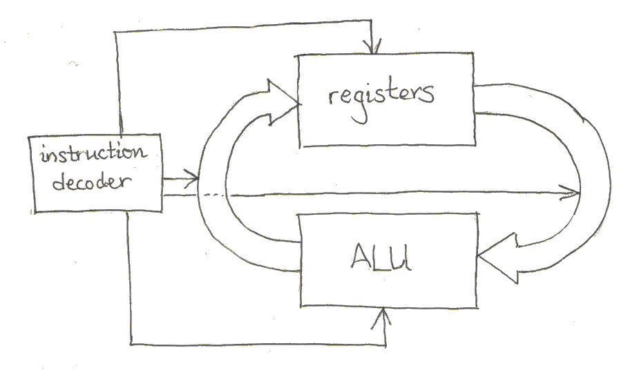
The registers store state, and are the only component which does this. Registers are designed so that their input and output are decoupled: changing the input data to a register doesn’t change the output data, until the register is both enabled for write, and a clock tick happens.
The ALU (arithmetic and logic unit) operates using only combinatorial logic1, and will take one or more inputs, and generate one or more outputs. In this design, I’m including the memory and I/O interfaces as part of the ALU (because I’m designing for synchronous memory).
Between the registers and the ALU is a bus (or several), which serves to move data from the registers to the ALU inputs, and from the ALU outputs to the registers.
The instruction decoder takes an instruction loaded from memory, and turns that into a set of control signals which connect registers to the ALU, and select options within the ALU.
Moving data with buses
Consider an addition operation: ADD x, y. This takes x and y,
and adds them together, and puts the result into x. So we need to
move x and y to the ALU, and then move the result back to x. But
a bus can only move one value at a time. There’s some trade-offs we
have to make here: on one extreme, we could have three buses (one for
each parameter, and one for the result). At the other extreme, we
could have a single bus, and use registers to store the parameter
values. The first option is faster – it only takes one clock cycle to
feed all the parameters to the ALU and get the result out again. The
second option is conceptually simpler, but slower – it needs three
clock cycles to set the parameters and retrieve the result. It’s also
more expensive, because we need several extra registers.
In practice, I’m going to go with something in between. It’s going to
be helpful for other reasons to have a single temporary register, t.
If we do that, we can hook it directly into one input parameter of the
adder, and into the address lines of the memory/IO unit, and then we
only need two buses: one input and one output.
ALU Operations
What goes into the ALU? Well, we need to be able to add and subtract things – that’s the adder unit (which can do both operations, with small modifications). We need a simple shifter to handle the right-shifts. And we need something to handle getting data in and out of memory and I/O – the memory unit. The fourth thing, which seems relatively pointless but turns out to be quite useful, is a passthrough, which just connects it input parameter to its output. We can use the passthrough to move data directly between registers without modifying it.
Other registers: PC and PSR
We need two more full registers – the program counter and the instruction register – and a few more bits of state – the processor status register.
Program counter
The program counter, pc, is a register which holds the address of
the next instruction to execute, and which is normally incremented on
every instruction. It may also be incremented during processing an
instruction, if the instruction takes an 8-bit parameter (such as ADD x, #5 or OUT (k), x). Finally, pc may be set directly by an
instruction – in our case, by a JMP instruction.
Instruction register
The instruction register, ins, is simply a copy of the
currently-executing opcode. This is set at the beginning of executing
each instruction, and is used by the instruction decoder to control
what gets done for that instruction.
Processor status register
The processor status register, psr, consists of three bits of
data, which indicate whether the result of the last instruction was
negative (the N bit), zero (the Z bit), or resulted in a carry
(the C bit). The C bit is also used as input to the ADC, SBC
and RRC instructions. This isn’t connected to the buses, but instead
has direct connections to and from the adder and shifter.
Overview
Putting all of this together, we end up with a plan that looks like the picture below:
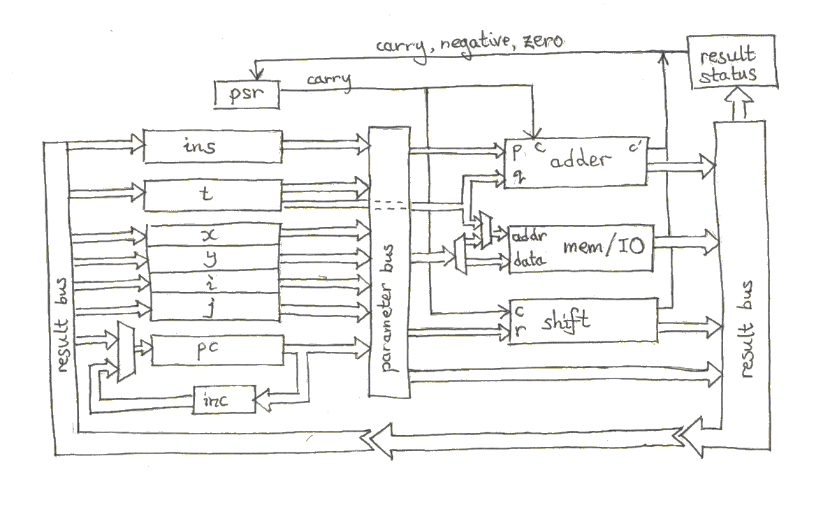
The seven main registers (of which four are accessible to the
programmer) are connected to a bus, which feeds a value from one of
the registers into into one of four processing units. The processing
units feed a result back into the registers. There are special
connections from the t register to the adder and the memory/IO unit.
There is a separate unit for incrementing the pc register, and
another for updating the psr bits.
“Above” this structure, and not shown here, the instruction decoder
reads from the ins register and sends control signals to all of the
components to ensure that they do things in the right order.
Conclusion
In this post, we’ve seen what the high-level components of the CPU are, and how they relate to each other. In the next post, I’ll start showing how the architecture in this post can be controlled, step by step, to execute the instructions we laid out in the first two parts, and go through some of the options for implementing the instruction decoder.
Go to the next post in this series.
-
Well, you could have an ALU that uses clock ticks and state registers internally for some operations, like multiplication. But I’m trying to keep things simple. ↩︎